At this point we have designed and tested VHDL for an adder datapath. We have also designed and characterized a standard cell library for the AMI C5N process. We now have enough to synthesize our VHDL designs using our cell library.
In a shell window, change to your synthesis work directory. There are two Synopsys setup files that you will need.
Copy ~jbakos/syn_work/.synopsys_dc.setup and ~jbakos/syn_work/.synopsys_vss.setup to your synthesis work directory.
Open .synopsys_dc.setup in a text editor and change the "designer" variable to your name and the paths for the "target_library" and "link_library" such that they BOTH point to your standard cell DB file.
Open .synopsys_vss.setup in a text editor. Observe the following line: ARITHMETIC_PARTS : ./ARITHMETIC_PARTS
This is a library mapping. In the future, you will need to add similar lines to this file for any library you use in your VHDL files. Don't forget about this!
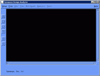
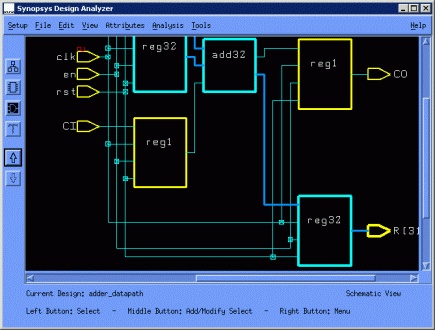
Now let's okay Synopsys. Type "design_analyzer" in your shell window. You should receive the following window.
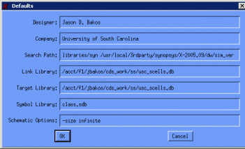
Select Setup | Defaults to verify that the settings in your .synopsys_dc.setup file have taken effect.
Let's begin reading our VHDL files in from the bottom of our hierarchy up. Let's start with the "bitadd" component. Select File | Analyze. Turn on "Create New Library if it Doesn't Exist". Type in "ARITHMETIC_PARTS" as your library. Browse to "[homedir]/HDS/my_project/arithmetic_parts/hdl" and double-click "bitadd_bitadd.vhd".
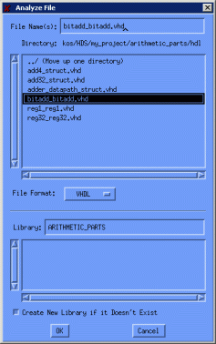
Repeat this same operation for the VHDL files containing your reg32, reg1, add4, add32, and adder_datapath components.
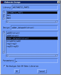
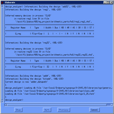
Now select File | Elaborate. Select the ARITHMETIC_PARTS library and the adder_datapath design. Click OK.
The following window will show you the results of the elaboration. Assuming there are no errors, you should see a similar window.
Your Design Analyzer window should now show the following designs.
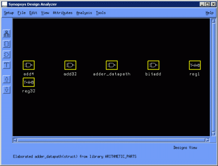
The components that have a gate symbol represent components whose behavior was simple enough to be instantly converted to a gate-level representation. The components that have a "Y=A+B" symbol represent components whose behavior is complex enough that they could not be instantly synthesized. This includes our registers, reg32 and reg1.
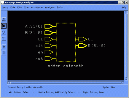
Double-click the adder_datapath component. You should see the interface for the component.
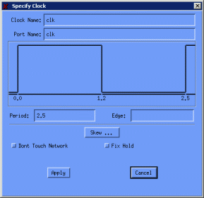
In order to perform timing optimization, you first need to tell Synopsys which pin is the clock pin. Click the "clk" pin to highlight it. Then select Attributes | Clocks | Specify. For the period, type "2.5", which tell tell Synopsys that we're targeting a 2.5 ns clock period, corresponding to a 400 MHz clock. Click Apply, then Cancel.
Now double-click on the component. This will show you the structure of the component. Zooming in is tricky with Synopsys. To do this, do a right-click in the window. This will bring up a pop-up menu. The tricky part is that you also need to use your right mouse button to choose an option from this menu. Then use your left mouse button to draw a zoom box. Synopsys will not show you the zoom box as your draw it, so you have to use your imagination. Hit Control-F to fit the design to the window.
You will also be able to double-click other components in the design to bring them up. In order to return open the interface view for the currently displayed design, you need to click the interface button, which is the second button down from the top on the left-hand toolbar. If you'd like to move up in the hierarchy, click the "up arrow" button, which is the second button up from the bottom on the toolbar.
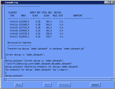
Let's perform a synthesis run and see if we can meet our timing constraint of 400 MHz. Return to the top-level design of the adder_datapath and select Tools | Design Optimization. Change the Map Effort to High and click OK.
Assuming that you didn't encounter any errors, synthesis will complete after a short computation period. Your log window should look similar to mine.
Use the up arrow button to return to the top. Your window should now look like the following.
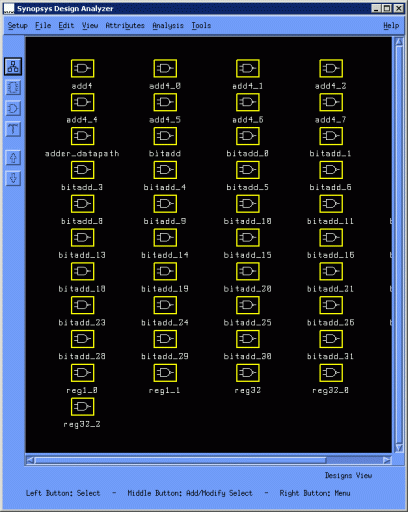
Design Analyzer has created a separate box for each component instance in your design. Let's check one of the reg1 instances, since this component was previously marked with the behavioral icon (before we optimized the design). Before you double-click it, you should already be able to see that the icon for reg32 and reg1 has been changed to the gate icon as a result of the design optimization. This indicates that these components are now cell-level (synthesized) designs. Double-click one of the reg1. Design Analyzer will initially bring up the interface description. Double-click the component again to see the cell-level design.
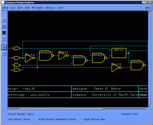
You can see that our DFFX1 cell is the core of this design, with several of our other gates added around the DFF in order to reconcile the differences in behavior between our VHDL reg1 component and our DFF cell (the addition of the synchronous reset input and the addition of the enable input).
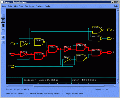
Open one of the bitadd components. This is the only purely gate-level combinational design because it doesn't contain any memory cells (all the other components are either sequential or hierarchical). Select Analysis | Highlight | Critical Path (or hit Control-T). This will show you the critical logic path through the circuit. In this case, the delay is 6 gate delays, which is roughtly equivalent to 6FO4. Note that this does not represent the total pipeline stage delay, as there is additional serial logic in this datapath, including logic feeding this circuit and logic consuming the outputs of this circuit.
Feel free to check out your other VHDL components to see how Synopsys converted the VHDL descriptions to schematics using only your cells.
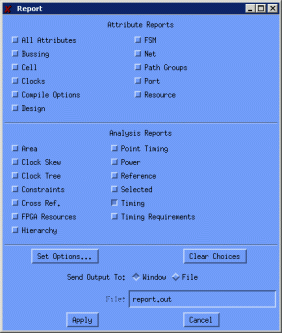
When you're done, return to the schematic for the adder_datapath (top-level schematic of your design). Select Analysis | Report. In the window, turn on Timing and click Apply.
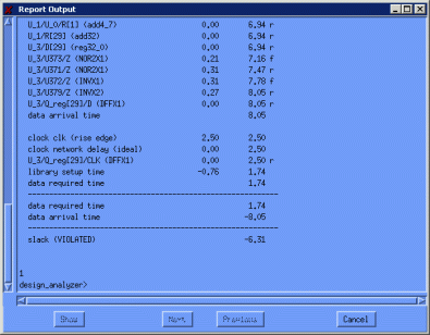
Click Apply. Scroll to the bottom of the window. As you can see, there was violated slack, meaning that the synthesized design did not meet our timing requirement.
Perform another design optimization and generate another timing report. You will see that the violated slack may be different (better or worse).
Unfortunately, sometimes the only way to improve these results is to make changes to your VHDL design (more efficient design, more pipelining, etc.).
For now, let's set a more realistic timing constaint. Go back to the interface of the adder_datapath, select the clk pin, select Attributes | Clocks | Specify. Enter 20 for the period and click Apply then Cancel.
Select Tools | Design Optimization and click OK. After synthesis, generate another timing report.
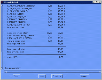
I ended up statisfying the 50 MHz clock (period of 20 ns) with 1.52 ns of available slack. What does this mean? After we place-and-route this design and determine the physical interconnect delays, these additional delays can only consume at most an additional 1.52 ns before the design will no longer satisfy timing. Are we cutting it close? We'll find out later.
Once you've done this, let's generate a timing constraint file for the next stage in the design flow. Select Setup | Command Window to open a command interface window. In the command window, type "write_sdc adder_datapath.sdc" and hit enter.
This script file will tell the place-and-route tool the name of the clock signal and specify our timing goal. The file is generated as follows:
		#####################################################

		#  Created by Design Compiler write_sdc on Fri Dec 30 14:04:28 2005

		#####################################################
		set sdc_version 1.4

		create_clock -period 20 -waveform {0 10} [get_ports {clk}]
Let's see how much area is required by our design. Select Analysis | Report. Turn off Timing and turn on Area. Click Apply.
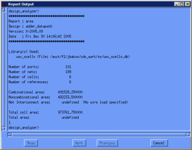
Our design requires 973.76175 mm^2.
In addition to timing, you can also set other design constraints for any component in the hierarchy. Do this by selecting Attributes | Optimization Constraints | Design Constraints. In this window, you can see constraints for area, dynamic power, leakage power, and maximum fanout. Under Attributes | Optimization Constraints | Timing Constraints, you can select input pins and output pins in any component in your hierarchy (using the middle mouse button to select pins) to set the associated maximum delay. You can also see the critical path for any circuit by selecting Analysis | Highlight | Critical Path. Note that the optimizer may or may not be able to meet these constraints. You will be able to verify that constraints were met by using the Report function.
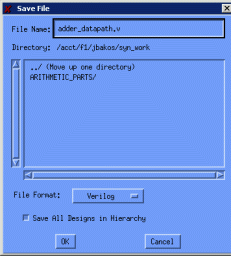
The next step in our design flow is to save our designs as a Verilog netlist, and to save the associated timing model using an SDF file. Go back to the design of the top-level component, which is adder_datapath. To save the netlist, select File | Save As. Change the file format to Verilog, and change the extension of the output file to ".v". Click OK.
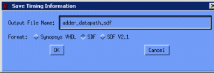
Now select File | Save Info | Design Timing. Change the format to SDF and the file extension to ".sdf". Click OK.
Open both files in a text editor. You will see that the Verilog netlist file is easy to read. For example, let's look at the module definition for the bitadd component.
		module bitadd_0 ( A, B, CI, G, P, S );
		  input A, B, CI;
		  output G, P, S;
		  wire   n33, n34, n35, n36, n37, n38, n39, n40, n41, n42, n43;

		  INV2X U45 ( .A(n34), .Z(P) );
		  INV U46 ( .A(n42), .Z(n33) );
		  NOR2 U47 ( .A(B), .B(A), .Z(n34) );
		  INV U48 ( .A(B), .Z(n42) );
		  INV U49 ( .A(A), .Z(n43) );
		  INV U50 ( .A(CI), .Z(n37) );
		  INV U51 ( .A(n38), .Z(n39) );
		  NAND2 U52 ( .A(n33), .B(n43), .Z(n36) );
		  NAND2 U53 ( .A(A), .B(n42), .Z(n35) );
		  NAND2 U54 ( .A(n36), .B(n35), .Z(n38) );
		  NAND2 U55 ( .A(n37), .B(n38), .Z(n41) );
		  NAND2 U56 ( .A(CI), .B(n39), .Z(n40) );
		  NAND2 U57 ( .A(n41), .B(n40), .Z(S) );
		  NOR2 U58 ( .A(n43), .B(n42), .Z(G) );
		endmodule
The format of this file is simple. The first four lines define the module name, interface, and internal signals. The main body is made up of lines in the following format:
Now let's take a look at the timing model (SDF) file.
This file has two sections. The first section defines the interconnect delays for every
physical wire in the design. You'll notice that all these delays are zero. This is because
the synthesizer has no knowledge of the technology or the physical layout of the circuits.
We will be generating another SDF file after we perform place-and-route of this synthesized
design. At this point, the place-and-route tool will know the physical interconnect lengths
and technology information to determine the interconnect delays (which are caused by
parasitic capacitance in the wires).
If you scroll down, you'll see the second section, which defines the delay associated with
each instantiated cell in the design. There are real numbers for these delays, because the
DB file contained characterization information for each cell, which included delay.
This timing model does more than assign a constant delay to each cell. The delays for each
cell depend on the fanout of each cell, which is dependant on how the design was synthesized.
Even when Synopsys tells us that we have met our timing constraints, we can perform simulation
at this point in our design flow to verify the functionality of the synthesized design and to
verify that our timing constaints have been met. We will use ModelSim for this.
In a shell window, switch to your synthesis work directory and type "vsim".
We're back in Modelsim. However, instead of compiled VHDL files, this time we'll be reading
in our Verilog netlist, our Verilog cell library, and the SDF delay model.
When ModelSim starts, close the information window.
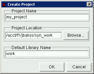
Select File | New | Project. Name the project whatever you'd like. Name the default library
"work". Click OK.
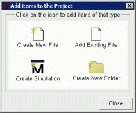
In the "Add items to the Project" window, click "Add Exisiting File".
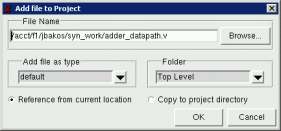
After this, browse-to and double-click your "adder_datapath.v" file. Then click OK.
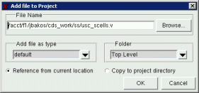
Again, click "Add Exisiting File". After this, browse-to and double-click your
"usc_scells.v" file (back in your SignalStorm work directory). Recall that this
is the Verilog cell library that we generated with SignalStorm. This library
contains the behavior of our cells as well as some timing information. Click OK.
After this, close the "Add items to the Project" window.
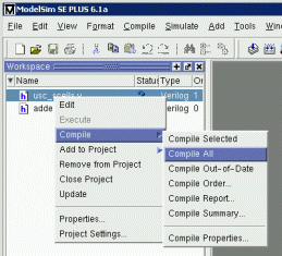
Do a right-click inside the Workspace pane and from the pop-up menu, select Compile | Compile All.
This will compile your Verilog files into Modelsim proprietary binary format.
After compilation, there should be checkmarks in the status column of the workspace pane.
Back in the main Modelsim window, select Simulate | Start Simulation. In the new window,
switch to the SDF tab. Click Add and browse to your SDF file in your synthesis work
directory.
Switch back to the Design tab, expand the work library (click the plus sign), select
adder_datapath, and click OK.
You will receive several warnings about unused module ports. This is happening because Synopsys
optimized away some of the signals in our design that aren't used. Examples of these in the 32-bit
adder include the carry-out outputs from all but the most significant 4-bit adder and the generate
and propagate from the most significant 4-bit adder. As such, it didn't even include connections
for the associated outputs on the 4-bit adders. This is okay, because Verilog modules are
instantiated using pass-by name parameters, so missing module output connections are okay.
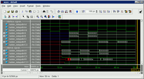
Open the wave window and add your signals just as you did before. Change the radix of all the
signals to hexadecimal.
Notice the timebase in Modelsim is now picoseconds instead of nanoseconds as before. This allows
for increased accuracy (resolution) in our simulation, which we need now that we're including latency
information in the design model.
We will setup our clock with a 20 ns period (50 MHz). A bug in the Modelsim GUI
prevents us from defining large periods relative to the timebase. To solve this problem,
we can simply use the command-interface command to setup the clock and explicitly specify
the time units for the period and duty cycle.
Issue the same sequence of ModelSim commands as in the last tutorial, but this time make
sure you explicitly specify your run lengths in nanoseconds (for example: "run 100 ns" instead
of "run 100"):
At this point, it is a wise idea to add these commands in a DO-file, since you will be repeating
this sequence of commands several times while varying the clock period. In other words, create
a "test.do" file containing the following script.
This way, you can make changes to the clock period/duty cycle, save the script, and rerun
it in Modelsim using the "do test.do" command.
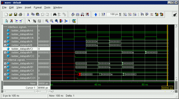
After you run this file, you should now see the following results. These results verify
both the functionality and the timing goals of the synthesized.
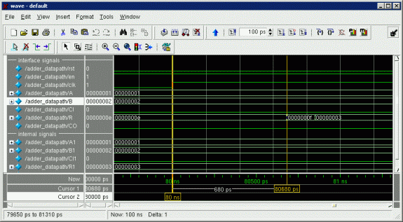
Zoom in on one of the rising edges of the clock signal. You can clearly see that our delay
model is being included in the simulation, as the output of the result register doesn't change
until 680 ps after the the rising edge of the clock. You can add a cursor in the wave window
by selecting Insert | Cursor and delete a cursor by selecting Edit | Delete Cursor.
Let's see if our design can operate with a 100 MHz clock. Change the second line of your
script to "force -freeze sim:/adder_datapath/clk 1 0, 0 {5 ns} -r 10 ns", and divide all
your run lengths by 2 (15, 10, 25).
Looks like we're okay at 100 MHz. Now let's try 400 MHz, which Synopsys claimed couldn't be
achieved with our design. Change the second line of your script to
"force -freeze sim:/adder_datapath/clk 1 0, 0 {1.25 ns} -r 2.5 ns" and divide all your
run lengths by 4 (3.75, 2.5, 6.25).
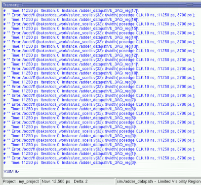
After the first "run" command, we see a sequence of errors in the Modelsim window.
The line being referenced in the error messages is the timing information for the DFF cell
(module) in the usc_scells.v file. This indicates that by increasing the clock speed to
400 MHz, we have violated timing requirements for the DFF cell.
Assuming that we have verified functionality and timing, we now have enough information to
place-and-route our design. Close Modelsim.
In the next tutorial, we will use the Verilog netlist to perform place-and-route.
Simulation for Functional and Timing Verification
force -freeze sim:/adder_datapath/clk 1 0, 0 {10 ns} -r 20 ns
		restart -f
		force -freeze sim:/adder_datapath/clk 1 0, 0 {10 ns} -r 20 ns
		force rst 1
		force en 1
		run 30 ns
		force rst 0
		force A X"00000004"
		force B X"0000000A"
		force CI 0
		run 20 ns
		force A X"00000001"
		force B X"00000002"
		run 50 ns