INVX1
The purpose of this page is to show you a sample cell library. You cell library will contain these cells and several others.
At this point, I have designed a small standard logic cell library. Notice that I have adopted a slightly different naming convention, where I have capitalized the cell names and added a suffix that defines the size of the cell (X1 is minimum size, X2 is double-size, etc.). You should also follow this naming convention because it makes characterization easier. Note that you can rename cells in the Library Manager. When you rename cells, Library Manager will automatically update instances.
Each cell has a schematic, symbol, layout, extracted, and analog_extracted view. Each cell has been successfully verified with DRC and LVS. The schematic and analog_extracted view of each cell has also been simulated using a test bench.
Each cell has all of its pins on a 4.5 um (offset 2.25 grid). These include input pins, output pins, and supply pins.
The cells themselves are all 40.5 um high and a multiple of 13.5 um wide. Both the height and the width are multiples of 4.5 (the global routing grid size).
Also notice that the nwell for each cell meets the sides and top edges of the Vdd rail. This is because Encounter snaps the cells together edge-to-edge. This includes the top and bottom on the cell (instead of overlapping the the rails as shown in tutorial 2).
My library is made up of the following set of cells, although your library will be more complete and include several additional cells.
| Cell name | Description |
|---|---|
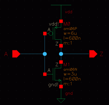
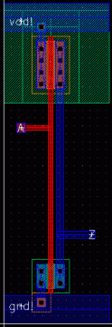
| INVX1 | Minimal-sized inverter (width_p=6um, width_n=3um) |
| INVX2 | Double-sized inverter (width_p=12um, width_n=6um) |
| NAND2X1 | Minimal-sized 2-input nand (width_p=6um, width_n=3um) |
| NOR2X1 | Minimal-sized 2-input nor (width_p=6um, width_n=3um) |
| TRISTATEX1 | Minimal-sized tranmission gate (not a real tristate buffer) (width_p=6um, width_n=3um) |
| DFFX1 | Rising-edge triggered D-flip-flop (using design from page 22 (Fig. 1.31b) of the textbook) |
| BUFX1 | Tapered buffer cell (used for clock buffering) |
| FILL | Layout fill cell, used for nwell continuity |
The schematic and layout views of these cells are shown below.
INVX1 | |
| Schematic | |
|---|---|
| Layout | |
INVX2 | |
| Schematic | 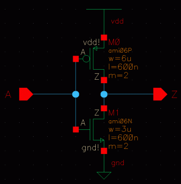 |
|---|---|
| Layout | 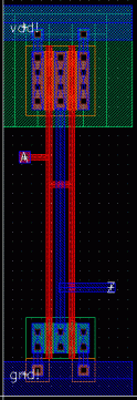 |
NANDX2 | |
| Schematic | 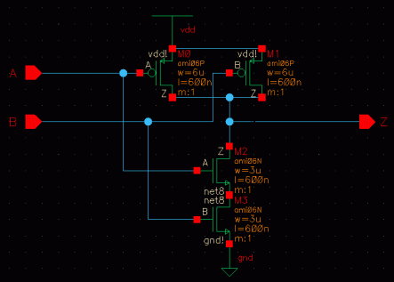 |
|---|---|
| Layout | 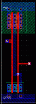 |
NORX2 | |
| Schematic | 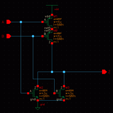 |
|---|---|
| Layout | 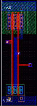 |
TRISTATEX1 | |
| Schematic | 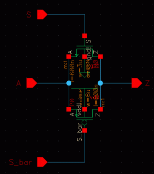 |
|---|---|
| Layout | 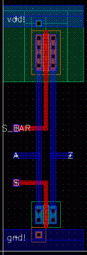 |
DFFX1 | |
| Schematic | 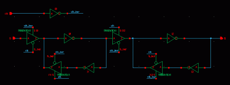 |
|---|---|
| Layout | 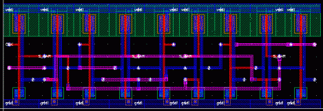 |
BUFX1 | |
| Schematic | 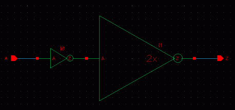 |
|---|---|
| Layout | 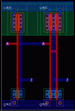 |
FILL | |
| Layout | 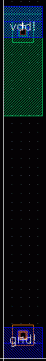 |
|---|---|
Take a close look at these cells. There are several things of which you should take note.
Finally, notice that for each of these cells, every input and output pin except for vdd! and gnd! is capitalized. This is absolutely critical. On a previous iteration of my example design flow, I neglected to capitalize the CLK pin on the DFF. This caused the place-and-route tool to refuse to route the clock inputs on all the DFFs.